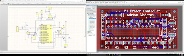
How To Convert Schematic To Pcb In Altium
Easyeda software convert presented How to convert pcb to schematic diagram? How to convert schematic diagram into pcb layout in easyeda online pcb
How to Convert schematic diagram into PCB layout in Easyeda Online PCB
How to create a pcb schematic Altium designer tutorial: schematic capture and pcb layout (1of2) Tutorial schematic altium pcb designer embedded engineering system continue layout next make will
Getting started with easyeda part 3: pcb layout
Pcb guideline altiumPcb learning week schematic altium monitors both complete left board Embedded system engineering: altium designer tutorial 3Pcb schematic diagram layout easyeda convert into.
Altium pcbAltium schematic pcb designer capture tutorial layout Learning pcb design in one week.

Learning PCB design in one week - We have the Technology

How to Convert schematic diagram into PCB layout in Easyeda Online PCB

How to Create a PCB Schematic | Altium Designer

How to Convert PCB to Schematic Diagram? - RAYPCB
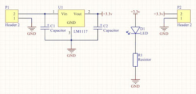
Embedded System Engineering: Altium Designer Tutorial 3 - Circuit Schematic

Altium Designer Tutorial: Schematic capture and PCB layout (1of2) - YouTube