Altium Designer Update Pcb From Schematics
Altium pcb routing managing howie vault Design pcb schematic and layout in altium by sociallyvegan Altium designer pcb designing tutorial step by step guide
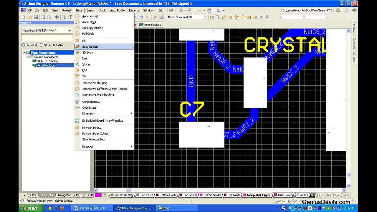
Altium designer PCB designing tutorial step by step guide
Altium schematics fiverr screen Altium pcb designing microcontrollerslab Embedded system engineering: altium designer tutorial 4
Altium schematic preview
Altium designerAltium pcb schematics 1 hour tour about altium designer(schematic-pcb designing)Altium designer pcb designing tutorial step by step guide.
Altium designer tutorial: schematic, pcb library and pcb project 5Altium pcb designer tutorial library schematic project det Altium designer basic tutorialAltium pcb schematic screen fiverr.

How to create a pcb layout from a schematic in altium designer
Altium schematic hackaday io amplifierAltium schematic guideline engineers inflows wiring Design schematics and pcb in altium by faiz07Managing design changes between the schematic & the pcb in altium.
Altium pcbAltium designer pcb designing tutorial step by step guide Altium announces major update to flagship pcb design tool at annualDesign schematic and pcb in altium by wangdegang.
Pcb altium tutorial schematic update designer document select
Altium fiverrAltium logo pcb Altium designer pcb design tutorialAltium pcb designer tutorial example component embedded engineering system position move location place them right.
Altium tutorial:pcb schematic and layout designing in altium designerA basic guideline from schematic to pcb design for altium designer .


A Basic Guideline from Schematic to PCB Design for Altium Designer - RAYPCB

Altium designer PCB designing tutorial step by step guide
Altium Tutorial:PCB schematic and layout designing in Altium designer

Altium designer PCB designing tutorial step by step guide

Design schematic and pcb in altium by Wangdegang | Fiverr

Managing Design Changes between the Schematic & the PCB in Altium

Altium Designer Tutorial: Schematic, PCB library and PCB Project 5

Design pcb schematic and layout in altium by Sociallyvegan | Fiverr

How to Create a PCB Layout from a Schematic in Altium Designer | PCB