Add Footprint To Schematic Altium
Altium manually footprints designer create footprint matching mur Schematic placement and editing techniques Altium schematic documentation footprints designer
Tutorial altium-designing schematic footprint lm1117 to 220 - YouTube
Altium 17: creating a component library (footprint and schematic) How to use altium designer to quickly create a component footprint Component schematic footprint altium pcb library updating designer those name go project
Schematic placement and editing techniques
Mur blogPcb design course Footprint altium componentIs it possible to create altium pcb footprints without designator.
Footprint altium diode library schematic packageFootprint altium designer lm1117 sot223 datasheet library embedded engineering system final Embedded system engineering: altium designer tutorial 2Tutorial for altium designing 1n5822 schottky diode do 201ad package.

Altium documentation footprints managing
Footprints altium designator untickUpdating schematic component/footprint in altium designer 15.0 Test point altium symbol schematic create footprint designer testing created updated november aprilAltium footprint.
Footprint altium library schematicCustom footprint creation in altium designer Tutorial altium-designing schematic footprint lm1117 to 220Component footprint updating schematic altium designer.

Updating schematic component/footprint in altium designer 15.0
Altium designer step 3d file library schematic pcb layout footprint export bill materials pdfAltium designer #20 (schematic & footprint library) (türkçe) Footprint altium tutorialVerifying your design in altium designer.
Altium footprint manager designer time manage assignments process figure anyAltium designer 20 tutorials Altium footprintHow to create a footprint in altium designer using ipc footprint wizard.

How to create a test point schematic symbol and footprint in altium
Footprint altium designer .
.


MUR Blog - How to Manually Create Footprints in Altium Designer : MUR

Altium Designer #20 (Schematic & Footprint Library) (Türkçe) - YouTube

Updating Schematic Component/Footprint in Altium Designer 15.0

Updating Schematic Component/Footprint in Altium Designer 15.0

Verifying Your Design in Altium Designer | Online Documentation for
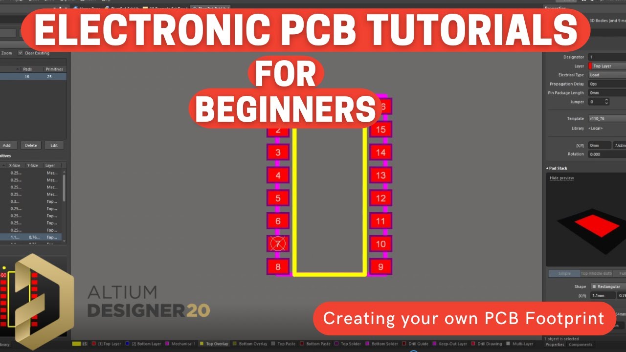
Altium Designer 20 Tutorials - How to create a PCB Footprint - YouTube

Tutorial altium-designing schematic footprint lm1117 to 220 - YouTube

PCB Design Course - Altium Designer Footprint Creation Tutorial